Practical Issues with IBIS Models
Bob Ross, Interconnectix Unit of Mentor Graphics Corporation
10220 S.W. Nimbus Avenue, K4, Portland Oregon 97223
Phone: (503) 603-2523, FAX: (503) 639-3469 E-mail: bob@icx.com
(Chair., EIA IBIS Open Forum)
INTRODUCTION
Printed circuit board design for dense, high-speed digital circuits requires layout tools to be used with electrical board analysis tools. Many Electronic Design Automation (EDA) vendors supply such tools to deal with signal integrity, timing and other design issues. Such tools require electrical models to describe the board components.
The I/O Buffer Interface Specification (IBIS), also known as ANSI/EIA-656, has become widely accepted among EDA vendors, semiconductor vendors and system designers as the format for digital electrical interface data. Spice models have often been requested for these purposes, but semiconductor vendors are now reporting more customer interest in IBIS models.
To illustrate its wide-spread adoption, at least four EDA vendors of PCB design tools accept the IBIS format directly, and all other significant vendors (including several Spice vendors) provide translation paths from IBIS into their internal formats. Because IBIS models do not reveal proprietary internal process or architecture information, semiconductor vendor’s support of IBIS continues to grow. Several methods exist to develop IBIS models, and consequently IBIS models can be provided from several sources, including the user. Finally, the IBIS format has proven useful to give reliable and accurate board-level simulation information.
Since 1993 IBIS has evolved from Version 1.0 to the current Version 3.0 to keep up with digital circuitry advances and simulation needs. The IBIS document has grown from 8 pages describing the core aspects to over 50 pages describing VERY PRACTICAL extensions and improvements. Unfortunately IBIS is now difficult to understand. We need to step back and communicate the essentials of IBIS and what constitutes good modeling practice.
This presentation provides both an overview of the fundamentals of IBIS and also gives some specific details of interest to IBIS users and developers. Topics include:
IBIS HISTORY
In the early 1990s, Intel Corporation initiated internally a Lotus spread-sheet table-based model while attempting to convey the stringent requirements of PCI bus drivers and provide a common format between divisions for external communication. Several vendor specific formats did exist at that time. Because data preparation and model availability had been primary issues, Intel invited EDA vendors to join forces and define a common model format. IBIS Version 1.0 was issued in June 1993 and a clarification update Version 1.1 in August 1993. The IBIS Open Forum dedicated to keeping abreast with technical needs and promoting the availability of IBIS models also was born.
IBIS Version 1.1 was introduced with the understanding that it would be expanded in an upward compatible manner. More EDA vendors, semiconductor vendors and users joined the IBIS Open Forum, and through their cooperative efforts IBIS Version 2.0 was presented June, 1994 with many technical
extensions. In February 1995, the IBIS Open Forum formally affiliated with the Electronic Industries Alliance (EIA). With some minor technical and textual clarifications and through formal letter ballot review processes, IBIS Version 2.1 was issued and became an official American National Standard Institute standard ANSI/EIA-656 in December 1995. Version 2.1 has remained until now as the next stable level of functionality.
The EIA IBIS Open Forum has continued meeting regularly for additional technical extensions. It has also been working on all aspects of promoting IBIS models, utilities and information. As a result the EIA IBIS Open Forum maintains an abundance of information, articles and helpful documents on the official EIA IBIS home page. Over 13 semiconductor vendors offer IBIS models directly and several commercial IBIS model vendors have up to 10, 000 components modeled. Spice to ibis, ibis_chk and IBIS plotting utilities have been developed for free availability. Several "IBIS Summit" meetings have been held to communicate new applications and ideas. The IBIS mailing lists are used to conduct business and also to provide a forum for questions and user issues. As a result of the collaboration of common interests, IBIS Version 3.0 has just been issued in June, 1997 to define the newest level of technical functionality.
Like Spice models, IBIS models are formatted in human-readable, ASCII text. However, IBIS models do not require proprietary information. The critical electrical characteristics are based on derivative information -- derived by simulation or measurement. Consequently, models of current devices are becoming more readily available in IBIS than in Spice formats.
Spice models tend to be buffer centric; the model often represents one of several inputs or outputs of a buffer. IBIS models are component centric; the model describes all pins of the physical component. Physical databases used for large board designs provide suitable component footprint interfaces, ideal for the insertion of IBIS component models. Thus, EDA vendors support IBIS to integrate electrical components with physical data describing thousands of nets.
IBIS Version 1.1 - Core Model (June - August1993)
Version 1.1 of IBIS introduced the baseline architecture associated with most CMOS, BiCMOS and TTL technologies. Included were these features:
Header Information and end of the file are defined by using these keywords:
[IBIS Ver]
[Comment Char] (Could be redefined anywhere in the file)
[File Name]
[File Rev]
[Date]
[Source]
[Notes]
[Disclaimer]
[End]
One or more Components could be defined by using these keywords:
[Component]
[Manufacturer]
[Package] (default L_pkg, R_pkg, C_pkg)
[Pin] (pin number, signal name, model name, L_pin, R_pin, C_pin, and reserved words GND, POWER and NC to define which model is attached to each pin and it’s pin specific package lead)
Each Model referenced by the [Pin] keyword could be defined by using these keywords:
[Model]
[Voltage Range]
[Pulldown]
[Pullup]
[GND Clamp]
[POWER Clamp]
[Ramp] (dV/dt_r and dV/dt_f ratios)
Figure 1 illustrates the electrical model including the C_comp subparameter with the default package model of an I/O buffer that might be referenced by the [Pin] keyword and defined under the [Model] keyword. Appendix 4 contains an actual IBIS file (with some Version 2.1 features).
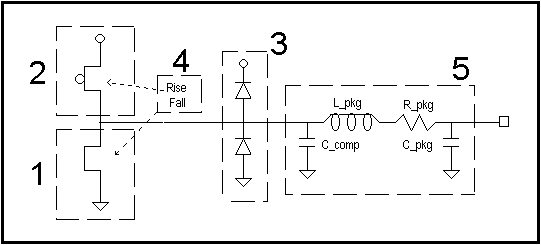
Figure 1. IBIS Version 1.1 Electrical I/O Buffer
Blocks 1 and 2 show output transistors that are modeled by DC I/V tables under the [Pulldown] and [Pullup] keywords.
Block 3 also consists of DC I/V tables [GND Clamp] and [POWER Clamp] representing the ESD or clamping diodes. When present, these diodes clamp transmission line reflections.
Block 4 shows the transition time of the output as it switches from one logic state to another. Rise and fall times are represented separately under the [Ramp] keyword as non-reduced ratios of transition voltage to transition time: dV/dt_r and dV/dt_f. In Version 1.1, this data is extracted under a load of 50 ohms. In later versions of IBIS, the load resistance can be selected.
Block 5 represents the pad and package parasitics seen by the output buffer. C_comp is the total output capacitance due to the output pad, clamp diodes and (for I/O structures) input transistors. L_pkg, R_pkg and C_pkg are the default inductance, resistance and capacitance of the bond wire and pin combination of the package. Pin-specific package parameters would be nomenclated: L_pin, R_pin, and C_pin.
Models of just input pins need only Blocks 3 and 5.
In IBIS Version 1.1, the [Voltage Range] actually defined the single supply voltage "Vcc" relative to ground. The [Pullup] and [Power Clamp] tables were made relative to Vcc. The [Pulldown] and [GND Clamp] table were made relative to ground.
These electrical characteristics are derived under defined test conditions from Spice model simulations or from device measurements. Spice models often contain process variations and allow simulations under temperature and supply extremes. The IBIS format groups corner descriptions into three columns: "typ" (typical), "min" (weak, slow) and "max" (strong, fast). These corners are defined with respect to process, pre-defined temperature and supply variations.
For the purposes of understanding the Core model and extensions, we can classify the key aspects into these areas:
In IBIS Version 1.1, the Information and Specification elements are in the Header section (See Appendix 1) and also listed as the following subparameters under [Model] (See Appendix 2 and Appendix 3):
Polarity: (Non-Inverting, Inverting)
Enable: (Active-High, Active-Low)
Model_type: (Input, Output, 3-state, Open_drain, I/O)
Vinh and Vinl threshold voltages (specification values, not actual values)
These subparameters are not included in Spice models, but useful for board-level signal integrity applications.
Version 2.1 (ANSI/EIA-656) - Practical Extensions (June 1994 - December 1995)
As EDA vendors began adopting the IBIS format and applying it to real designs, its practical limitations became apparent. Overcoming them led to these extensions:
A keyword to copyright files was added to the Header for completeness:
[Copyright]
Under the [Component] keyword, three new keywords were introduced related to packages and pins:
[Package Model] (calls a model named under [Define Package Model])
[Pin Mapping] (associates pins and power and ground busses)
[Diff Pin] (associates differential I/O pins and defines differential thresholds)
Under the [Model] keyword, more detail was added via new keywords:
[Temperature Range] (actually for information)
[Pullup Reference] (for individual I/V table references)
[Pulldown Reference]
[POWER Clamp Reference]
[GND Clamp Reference]
[Rgnd] (for terminators)
[Rpower]
[Rac]
[Cac]
[Rising Waveform] (for transition detail accuracy)
[Falling Waveform]
The set of Model_type variables were extended to include:
Open_sink (same as Open_drain)
Open_source
I/O_open_sink and I/O_open_drain
I/O_open_source
Input_ECL (for ECL and PECL technologies)
Output_ECL
I/O_ECL
Terminator (for terminator models including clamps)
Timing specification subparameters were added to define timing test loads and measurement points under the [Model] keyword to correlate calculated delays with specification delays:
Cref
Rref
Vref
Vmeas
Under the [Ramp] keyword, the subparameter R_load was added to define the test load for the dV/dt_r and dV/dt_f transitions.
A major package model expansion for supporting a single section of coupled pins was introduced with keywords shown in Appendix 1 under Package Model Definition. This extension allowed the package model to be defined within a .ibs file or within a separate .pkg file using the same header and end of file keywords. The format for package matrices included Full_matrix, Banded_matrix, and Sparse_matrix. These formats provided the self and coupled elements for all pins.
Version 3.0 - More Extensions and Refinements (June 1997)
IBIS Version 3.0 has just been ratified on June 1997 by the EIA IBIS Open Forum to continue to address the practical needs of current designs. Its additions include:
New [Component] keywords are introduced for series pin associations and for selecting different models:
[Series Switch Groups] (for associating series pins and series switch states)
[Series Pin Mapping]
[Model Selector] (for selecting one of several models)
Two subparameters for the [Component] keyword were introduced to allow specifying test point location for ASICs and other devices for signal integrity and timing:
SI_location (Die or Pin)
Timing_location (Die or Pin)
New [Model] keywords added specification and electrical detail associated with multi-staged drivers, diode kickback and series and series switch devices:
[Model Spec] (an extensive specification enhancement including typ-min-max values,
hysteresis, overshoots and pulse immunities)
[Driver Schedule] (multi-staged switching consisting of sequenced drivers)
[TTgnd] (diode kickback parameters)
[TTpower]
[On] (series switch state demarcations)
[Off]
[R Series] (discrete series elements)
[L Series]
[Rl Series]
[C Series]
[Lc Series]
[Rc Series]
[Series Current] (series I/V table)
[Series MOSFET] (series switch model)
Two new Model_types are defined to be associated with the above keywords:
Series
Series_switch
The Version 2.1 package model was extended as shown in Appendix 1 to include section of discrete or transmission line elements and also stubs for ballgrid arrays.
Also an Electrical Board Description with keywords shown in the Appendix 1 was introduced to extend the IBIS format usage to multi-board analysis. Its contents along with the Header and end of file information are formatted in a separate .ebd file.
Semiconductor vendors now are issuing IBIS models with some of the Version 3.0 features, and EDA vendors have already included some of the features and are working on others. IBIS Version 2.0 took about three years for full acceptance, and we are now starting the new cycle for Version 3.0.
THE MODELING PROBLEM
Model availability has consistently been a serious user issue. A number of options now exist, but the user will still be burdened with (1) qualifying models which are provided, and (2) generating models which are not.
Where Do You Get IBIS Models?
CAE vendors generally do not intend to provide "commercial" quality libraries. Instead, they provide a selection of representative devices or models for the user to stub into the design. Semiconductor vendors provide free models. Unfortunately, the quality of these offerings vary from bad to good, forcing the user to qualify the models. Sometimes for historical reasons and lack of understanding, the data is bad, and other times the data is incomplete. Commercial vendors provide a more consistent set of models and have the opportunity for providing the highest quality models. The quality is also quite variable. Often the design calls for devices that do not have IBIS models. The user then must apply pressure to get the model from the semiconductor Vendor, contract its development through commercial Vendors, or developing it him/herself. In all cases the user needs to qualify any model and may even need to extend an existing model to make it suitable for the intended usage.
What is the most basic model you can produce?
You can still estimate a buffer model with a fixed series resistor and a voltage source of the approximate rise and fall times for the device and format this information into an IBIS syntax. For board simulation with transmission line interconnects, you will still get the fundamental characteristics of the actual device under simulation. EDA simulators will still show reflections on the net due to loads distributed on the net and the characteristics at the driver pin should be approximately correct. In most cases, you should learn enough from this fundamental model to determine if your design is valid.
How do you create IBIS Models?
Semiconductor vendors presumably have the best source information, either the Spice models or measurement plus the internal contacts for the latest releases and undocumented details. Commercial vendors rely on Spice information provided by the semiconductor vendors (along with internal relationships) or have measurement setups for consistent data extraction. One can argue that device-based models are not guaranteed to be "typical", but on the other hand, some of the supplied Spice information may not reveal the details of all of the buffers, or be the latest information. So good or bad
models can be generated for either source. Users may also have access to Spice models (not necessarily the best ones) or measurement setups that can be used to create IBIS models. Databooks and data sheets contain specification information needed to complete the model. Sometimes data books capture the necessary I/V data generating tables. This could also be used for I/V tables. However, some of this information is too generic and may not show the actual variations that exist in the device.Many users already have developed a model library for their existing (non-IBIS) simulator. IBIS formatted models can be translated from this data. However, the IBIS format tends to have additional information requirements which may needed to be added separately. Several CAE vendors offer non-public tools to translate (reformat) IBIS models to or from other simulator formats.
MODEL VALIDATION
To simply check out models that you are developing or that are available from others, you need to go through these steps:
Visual Inspection for Completeness and Reality
Are all pins modeled?
IBIS is component centric requiring it to be "plugged in", just like a component.
Are the data values realistic?
As a result of other conventions, the units for values are sometimes not correctly inserted. The IBIS format uses MKS units with only these CASE-SENSITIVE multipliers: T, G, M, k, m, u, n, p, f for tera-, giga-, meg-, kilo-, milli-, micro-, nano-, pico-, and femto-, respectively. All other characters and additions to the first character (e.g., pF, V) are accepted and are not processed. We would visually expect to see capacitances of the order of pF, inductances, nH, resistors, ohms to milliohms, currents milliamperes, and time in nanoseconds in the database. Note, scientific notation is allowed, so check on the reality of the values.
Is the necessary information provided for your simulation?
Some early Version 1.1 level IBIS models do not include all of the voltage threshold values for Inputs and I/Os. While the model passed the ibis_chk utility for Version 1.1, because they were not required (this is changed in Version 2.0 and above), the thresholds are really needed for most board level simulators. Similarly, the timing test load information in IBIS Version 2.1 (Vmeas, Rref, Cref, Vref) often omitted is required by several simulators which also work with timing rules and databases. This Specification information should be inserted.
Model Checking (ibis_chk)
The IBIS Open Forum Committee has funded the development of the ibis_chk utilities for Version 1.1 and Version 2.1. It is currently contracting the development of a Version 3.0 checker. These utilities check for correct IBIS model format. They can also function as IBIS parser and translator front ends. An ibischk2+ developed by Quad Design (now Viewlogic) extends the checking capability by issuing more Warnings for suspicious model data. The executables are publicly available at no charge.
The latest utility ibischk2+ is the best one to use. It embeds the original ibis_chk utility directly for Version 1.1 level checking. However, we strongly recommend that if the model is designated Version 1.1, change the [IBIS Ver] to 2.1 and use ibischk2+. Not only will you get a much more detailed set of checking, you will get some Warning and Error messages for threshold omissions, for non-monotonic tables (this is allowed, but BE WARNED that certain types will cause serious problems in many simulators), and for suspicious data.
Graphical Inspection Using s2iplt or winibis
There are two publicly available utilities for viewing the tables of IBIS models. North Carolina State University developed a Perl and GNUPLOT based s2iplt utility suitable for Unix based applications.
HyperLynx offers winibis at no charge their Visual IBIS Editor for viewing, checking and editing IBIS files at the Version 1.1 and Version 2.1 levels. Many other companies provide their own IBIS development, viewing, and translation tools and products.
While it will take experience to view what is realistic, there are some obvious thing to look at.
Discontinuities and Extrapolation
Be suspicious of data with abrupt discontinuities. Even if it is valid, it will probably not simulate correctly. One way of working around this may be simply to truncate the data at the discontinuity. Most behavioral simulators linearly extrapolate the data points based on the last two data points. So reasonable simulation will still be assured with truncated data. However, look at the endpoints of the clamping tables in particular regarding any unintended slopes that can be extrapolated. Typically, two successive 0 mA values in the tables will solve this problem.
Non-monotonic Data
As a result of the existing s2ibis extraction algorithms and correct mathematical interpretation of the specification, the [Pullup] and [Pulldown] table may show data curving back to 0 A in the clamping regions. For many simulators this is acceptable because the clamping data that also exists has been subtracted from the [Pulldown] or [Pullup] data. It will be added again to produce a monotonic table. The foldback is a result of the numerical artifact of subtracting two large values to produce a small value.
Other non-monotonic behavior is likely to cause problems. Some of it is a result of older version s2ibis extraction tool bugs. A [Pulldown] table that starts to fold back to 0 mA as the voltage increases usually needs to be truncated. Even minor non-monotonic behavior that actually exists may still need to be truncated - with negligible loss of accuracy.
Clean Time Responses
IBIS level Version 2.1 models often include waveform information. IBIS Version 2.1 gives a large amount of latitude in setting up the loads for the extraction. Some of the loads do capture actual simulation characteristics, but the data itself does not yield a model that gives a good simulation. As a rule, the more additional information added, the more information has to be de-embedded (with loss of accuracy). Capacitive and inductive loads and fixture package parameters should be avoided. They will produce slower responses and possibly introduce ringing in the response. If there is excessive ringing, the best solution is simply to delete the data.
A second problem is that IBIS requires the beginning and ending values of waveforms to converge to their final values. The ibischk2+ utility provides a Warning if this is not achieved to within 2%. The graphical representation may also visually show that the waveform has not reached its final value. A larger simulation time window should have been used to extract the data.
Remember, the model should use data that will produce the BEST SIMULATION model that works with the SIMULATORS of choice. The best model is NOT likely to be the one that captures the unusual simulation artifacts and extreme test conditions. Rather, the best model is likely to be the one that captures the most typical conditions and extraction situations which yield the cleanest set of parameters.
Simulation
The final test is to actually use the IBIS model in a simulation and to observe whether the response is realistic in terms of transition times and voltage levels.
MODEL DEVELOPMENT ISSUES
This section covers some of the current issues the user may encounter.
Spice to IBIS
North Carolina State University under ARPA funding and with EDA vendor participation has generated some public domain Spice to IBIS translators and a utility for viewing IBIS files. These can be used directly or can be adapted to specific semiconductor vendor Spice formats. The source code and executables are available at no charge. Two utilities with different syntax are s2ibis_ver1.3 and s2ibis2_ver1.1. These utilities are set up for Berkeley 2 and 3 Spices, PSpice and HSPICE and Spectre. One advantage is that they produce syntactically correct IBIS models of levels 1.1 or 2.1.
The utilities are not easy to use and still require some fixes. They require average knowledge of Spice to sort out the unique features of Spice models including subcircuit construction and parameter passing. IBIS Version 2.1 contains a lot of features that can be handled by s2ibis2, but this adds to the complexity.
The user sets up (for the given syntax) the s2ibis control deck. This deck links into the Spice model (usually a subcircuit). When s2ibis is executed, the control deck sets up a large number of Spice decks for a variety of I/V table extractions and for time response extraction under typical, minimum, and maximum conditions. For just ONE buffer, this can result in 18 or more such Spice decks! Each of these decks is executed and the output table data is saved. The s2ibis utility then takes the data, processes it where necessary and stores it into the appropriate locations within the IBIS format.
The main difficulty is getting the Spice model to work and then to remove any built in input, and enable sources, any built in loads, built in package values, and any fixed voltage and temperature settings. The s2ibis control deck supplies the power, temperature, stimulus and load parameters.
There are EDA simulator vendor preferences, but the best waveform test loads tend to be in the purely resistive 50 ohm region, similar to the incident load in a transmission line environment.
The s2ibis utilities do not cover situations where internal pullup/pulldown "resistors" (usually FETs) exist. At this time the user needs to ignore the effect or to manually modify the models to avoid double counting. One company did include handling pullup/pulldown additions to their IBIS model generation program for ASICs because their internal Spice models had controls to include or exclude these pullup/pulldown elements.
Manual Model Development
If you need to develop a model from scratch of from table data, you need to understand some of the IBIS conventions regarding I/V table polarity. The automated utilities already do the correct translations. Refer to the IBIS Cookbook document for more detail.
One underlying principle is that the I/V tables are constructed relative to and offset from some defined Voltage. For standard CMOS/TTL technology, the I/V tables for [GND Clamp] and [Pulldown] are relative to the lowest voltage (typically ground), and [POWER Clamp] and [Pullup] are relative to the highest voltage (typically Vcc). However, the offsets for [POWER Clamp] and [Pullup] are "polarity reversed" according to the formula Vtable = Vcc - Vmeasured. One way of reading these table is to mentally reverse the voltage sign of the table and add that value to Vcc.
Furthermore, for ECL technologies the [Pulldown] table is made relative to the highest voltage (usually 0 V for ECL, Vcc for PECL), and it is also constructed in a polarity reversed manner. So when manually inserting IBIS table data, be aware of these conventions. You can also use a correct, existing IBIS model as a template.
Insertion of Additional Information
As previously mentioned the threshold information Vinl and Vinh is virtually required for Inputs and I/Os by all simulators. In addition, the timing test loads may be needed. This information is available form databooks and data sheets.
Other Extensions
Differential Models require the [Diff Pin] keyword to provide the association. The timing test load for differential pins will still be the single ended test load (even if it is the approximate Thevenin equivalent.
Some, but not all, simulators process the [Pin Mapping] keyword to describe ground and power busses for added ground and power bounce accuracy and SSO (simultaneous switched outputs) detail.
Version 3.0 extensions are important. However, you need to check what the simulator currently supports and what you need for your analysis. The primary support for Version 3.0 extensions will come from the EDA vendors as Version 3.0 features are adopted and from semiconductor vendors who already are issuing, out of necessity, IBIS models with certain Version 3.0 features. Because some of the details can be quite technical, the Version 3.0 features are not discussed here.
FUTURE DIRECTIONS
Models and Web Sites
The EIA IBIS Open Forum supplies information and development tools and promotes IBIS model development and distribution by all sources. Forum data can be accessed under http://eda.org/pub/ibis. It contains the complete IBIS repository: tools (ibis_chk and Spice to IBIS utilities), models, meeting minutes, e-mail archive, working documents, issues documents (BIRD for Buffer Issue Resolution Document), rosters, contacts, and other descriptive documents (Cookbook, Overview, articles). The EIA IBIS Open Forum home page is http://eia.org/eig/ibis/ibis.htm. It links to member company home pages and links to IBIS models, frequently asked questions and other IBIS related information.
International Interest
IBIS is already referenced in the Electronic Design Interchange Format EDIF Version 4 0 0. IBIS Version 2.1 has been put forth as a new work item in the International Electrotechnical Commission (IEC) as 93/46/NP. A French proposal is under consideration under IEC for "IBIS Modeling and EMC Simulation" as 93/60/NP. Finally, a more detailed extension and hybrid of IBIS and Spice syntax for buffers and packages is being considered by the Electronic Industries Alliance of Japan (EIAJ). They propose a nodal based structure while preserving the table-based electrical characterization methodology of IBIS.
EIA IBIS Open Forum Support
The EIA IBIS Open Forum continues with active participation and should be considered for technical support. Telephone conference call meetings are conducted every third week. Two face-to-face meetings are scheduled in conjunction with the Design Automation Conference and the DesignCon (formerly known as Design SuperCon) shows. In 1997 alone, over 60 people representing over 35 companies have participated. More than 20 companies hold formal membership status. The EIA IBIS Open Forum participants candidly exchange information. The ibis-users@eda.org reflector contains over 300 people to assist users. Official EIA IBIS business is conducted on the ibis@eda.org reflector. You may subscribe to these reflectors by sending your request to ibis-request@eda.org. Individual questions can be directed to ibis-info@eda.org. The ANSI/EIA-656 specification is available through Global Engineering Documents, (800) 854-7179.
APPENDIX 1 - TABLE OF IBIS KEYWORDS
HEADER SECTION
|
Version 1.1 [IBIS Ver] [Comment Char] [File Name] [File Rev] [Date] [Source] [Notes] [Disclaimer] |
Version 2.1 [Copyright] |
Version 3.0 |
[COMPONENT] PINOUT MODEL AND PACKAGE SELECTION
|
Version 1.1 [Component] [Manufacturer] [Package] [Pin]
|
Version 2.1 [Package Model] [Pin Mapping] [Diff Pin] |
Version 3.0 [Series Switch Groups] [Series Pin Mapping] [Model Selector] |
[MODEL] DEFINITION
|
Version 1.1 [Model] [Voltage Range] [Pulldown] [Pullup] [GND Clamp] [POWER Clamp] [Ramp]
|
Version 2.1 [Temperature Range] [Pullup Reference] [Pulldown Reference] [POWER Clamp Reference] [GND Clamp Reference] [Rgnd] [Rpower] [Rac] [Cac] [Rising Waveform] [Falling Waveform] |
Version 3.0 [Model Spec] [Driver Schedule] [TTgnd] [TTpower] [On] [Off] [R Series] [L Series] [Rl Series] [C Series] [Lc Series] [Rc Series] [Series Current] [Series MOSFET]
|
PACKAGE MODEL DEFINITION
|
Version 1.1
|
Version 2.1 [Define Package Model] [Manufacturer] (Ver 1.1) [OEM] [Description] [Number Of Pins] [Pin Numbers] [Model Data] [End Model Data] [Resistance Matrix] [Inductance Matrix] [Capacitance Matrix] [Row] [Bandwidth] [End Package Model] |
Version 3.0 [Number Of Sections]
|
ELECTRICAL BOARD DESCRIPTION
|
Version 1.1
|
Version 2.1
|
Version 3.0 [Begin Board Description] [Manufacturer] (Ver 1.1) [Pin List] [Path Description] [Reference Designator Map] [End Electrical Description] |
[END] OF FILE
|
Version 1.1 [End] |
Version 2.1
|
Version 3.0 |
APPENDIX 2 - TABLE OF [Model] SUBPARAMETERS
|
Version 1.1 Polarity (Non-Inverting, Inverting) Enable (Active-High, Active-Low) Model_type (See Appendix 3) C_comp (Values) Vinh (Value) Vinl (Value) |
Version 2.1 Cref (Value) Rref (Value) Vref (Value) Vmeas (Value) |
Version 3.0 |
APPENDIX 3 - TABLE OF [Model] SUBPARAMETER Model_type SELECTIONS
|
Version 1.1 Input Output 3-state Open_drain I/O
|
Version 2.1 Open_sink Open_source I/O_open_drain, I/O_open_sink I/O_open_source Input_ECL Output_ECL I/O_ECL Terminator |
Version 3.0 Series Series_switch |
APPENDIX 4 - SAMPLE IBIS MODEL
|**************************************************************************
|
[IBIS Ver] 2.1
[Comment Char] |_char
[File Name] n74f244n.ibs
[File Rev] 2.0
[Date] September 17, 1997
[Source] File originated at Intel Corporation, as an example of an
IBIS Version 1.0 file.
[Notes] This is modified from an original Version 1.0 example to
include some IBIS Version 2.1 features to illustrate some
keywords, subparameters and IBIS format style.
[Disclaimer] This information is for modeling purposes only, and
is not guaranteed.
[Copyright] None
|
|**************************************************************************
|
[Component] N74F244N
[Manufacturer] Philips
[Package]
| typ min max
R_pkg 50m 10m 100m
L_pkg 6.3nH 2.4nH 10.2nH
C_pkg 1.35pF 0.89pF 1.81pF
|
|**************************************************************************
|
[Pin] signal_name model_name R_pin L_pin C_pin
|
1 OEa# ENABLE NA 10.2nH 1.81pF
2 Ia0 F244_INP NA 7.8nH 1.50pF
3 Yb0 F244_OUT NA 5.8nH 1.17pF
4 Ia1 F244_INP NA 4.3nH 1.18pF
5 Yb1 F244_OUT NA 2.6nH 0.89pF
6 Ia2 F244_INP NA 2.4nH 0.89pF
7 Yb2 F244_OUT NA 3.3nH 1.18pF
8 Ia3 F244_INP NA 4.7nH 1.17pF
9 Yb3 F244_OUT NA 6.4nH 1.50pF
10 GND GND NA 8.9nH 1.81pF
11 Ib3 F244_INP NA 8.9nH 1.81pF
12 Ya3 F244_OUT NA 6.4nH 1.50pF
13 Ib2 F244_INP NA 4.7nH 1.17pF
14 Ya2 F244_OUT NA 3.3nH 1.18pF
15 Ib1 F244_INP NA 2.4nH 0.89pF
16 Ya1 F244_OUT NA 2.6nH 0.89pF
17 Ib0 F244_INP NA 4.3nH 1.18pF
18 Ya0 F244_OUT NA 5.8nH 1.17pF
19 OEb# ENABLE NA 7.6nH 1.50pF
20 Vcc POWER NA 10.2nH 1.81pF
|
|**************************************************************************
| F244_OUT MODEL
|**************************************************************************
|
[Model] F244_OUT
Model_type 3-state
Polarity Non-Inverting
Enable Active-Low
Rref = 500
Cref = 50pF
Vref = 0V
Vmeas = 1.5V
| Signals Ya(0-3),Yb(0-3)
| typ min max
C_comp 5.0pF 2.0pF 8.0pF
|
|**************************************************************************
|
| typ min max
[Voltage Range] 5.0V 4.5V 5.5V
|
|**************************************************************************
|
[Pulldown]
| Voltage I(typ) I(min) I(max)
|
-5.0V -16m -15.2m -16.5m
-4.0V -14m -13.2m -14.5m
-3.0V -12m -11.2m -12.5m
-2.0V -10m -9.2m -10.5m
-1.0V -8.0m -7.2m -8.5m
0.0V -5.5m -4.8m -6.0m
0.1V -5.0m -4.3m -4.5m
0.2V 0.0m -1.5m 6.5m
0.3V 25m 17m 35m
0.5V 100m 85m 110m
0.8V 215m 190m 230m
0.9V 245m 193m 270m
1.0V 260m 196m 300m
1.1V 265m 198m 320m
1.5V 276m 203m 350m
1.7V 280m 207m 357m
1.8V 282m 210m 370m
1.9V 295m 218m 385m
2.0V 310m 230m 400m
2.1V 325m 242m 417m
2.2V 340m 252m 431m
2.3V 348m 256m 440m
2.5V 356m 260m 450m
3.0V 378m 274m 465m
4.0V 431m 312m 510m
5.0V 485m 362m 560m
10.0V 755m 612m 810m
|
[Pullup]
| Voltage I(typ) I(min) I(max)
|
-5.0V 0.0m 0.0m 0.0m
1.1V NA NA 0.0m
1.2V NA NA -0.2m
1.3V 0.0m NA -2.2m
1.4V -0.5m NA -5.8m
1.5V -2.0m 0.0m -9.8m
1.6V -5.3m -0.8m NA
1.7V NA -2.5m NA
1.8V NA -6.9m NA
2.0V -26m -16m -35m
2.5V -52m -42m -61m
3.0V -78m -67m -84m
3.5V -102m -90m -105m
4.0V -124m -114m -124m
4.5V -143m -134m -143m
5.0V -162m NA -162m
5.5V NA NA -179m
10.0V -347m -299m -384m
|
[GND Clamp]
| Voltage I(typ) I(min) I(max)
|
-5.0V -784m -756m -811m
-1.0V -64m -56m -71m
-0.8V -29m -25m -33m
-0.7V -18m -14m -22m
-0.6V -8.0m -5.5m -11.5m
-0.5V -1.2m -0.3m -5.0m
-0.4V 0.0m 0.0m -0.5m
-0.3V 0.0m 0.0m 0.0m
5.0V 0.0m 0.0m 0.0m
|
|**************************************************************************
|
[Ramp]
| typ min max
dV/dt_r 1.5/2.00n 1.5/2.98n 1.5/1.61n
dV/dt_f 2.0/1.21n 2.0/1.74n 2.0/0.65n
|
|**************************************************************************
| F244_INP MODEL
|**************************************************************************
|
[Model] F244_INP
Model_type Input
| Signals Ia(0-3),Ib(0-3)
Vinl = 0.8V
Vinh = 2.0V
| typ min max
C_comp 4.0pF 2.0pF 6.0pF
|
|**************************************************************************
|
| typ min max
[Voltage Range] 5.0V 4.5V 5.5V
|
|**************************************************************************
|
[GND Clamp]
| Voltage I(typ) I(min) I(max)
|
-5.0V -699m -684m -718m
-1.0V -59m -54m -68m
-0.9V -44m -40m -52m
-0.8V -30m -27m -34m
-0.7V -18m -16m -23m
-0.6V -9.0m -6.8m -13m
-0.5V -2.8m -1.7m -6.0m
-0.4V -1.1m -1.0m -2.0m
-0.3V -1.0m -0.9m -1.1m
1.15V -145u -150u -138u
1.20V -145u -150u -100u
1.25V -90u -145u -37u
1.30V -48u -60u -8u
1.35V -10u -20u 0.0u
1.40V 0.0u -3u 0.0u
1.45V 0.0u 0.0u 0.0u
5.0V 0.0u 0.0u 0.0u
|
|**************************************************************************
| ENABLE MODEL
|**************************************************************************
|
[Model] ENABLE
Model_type Input
| Signals OEa#,OEb#
Vinl = 0.8V
Vinh = 2.0V
| typ min max
C_comp 4.0pF 2.0pF 6.0pF
|
|**************************************************************************
|
| typ min max
[Voltage Range] 5.0V 4.5V 5.5V
|
|**************************************************************************
|
[GND Clamp]
| Voltage I(typ) I(min) I(max)
|
-5.0V -1077m -1051m -1092m
-1.0V -77m -61m -82m
-0.9V -56m -43m -60m
-0.8V -39m -29m -43m
-0.7V -26m -17m -29m
-0.6V -16m -8.0m -19m
-0.5V -8.0m -1.8m -10m
-0.4V -2.5m -765u -3.8m
-0.3V -820u -680u -1.2m
-0.2V -710u -656u -780u
-0.1V -684u -637u -740u
0.0V -670u -620u -720u
1.60V -206u -223u -195u
1.65V -205u -222u -80u
1.70V -100u -221u -30u
1.75V -15u -220u -4u
1.80V -3u -200u 0.0u
1.85V 0.0u -40u 0.0u
1.90V 0.0u -4u 0.0u
1.95V 0.0u 0.0u 0.0u
5.0V 0.0u 0.0u 0.0u
|
|**************************************************************************
|
[End]