Date: Mon Mar 07 2005 - 08:43:35 PST
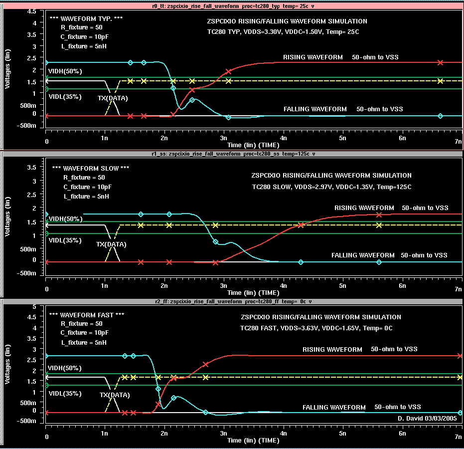
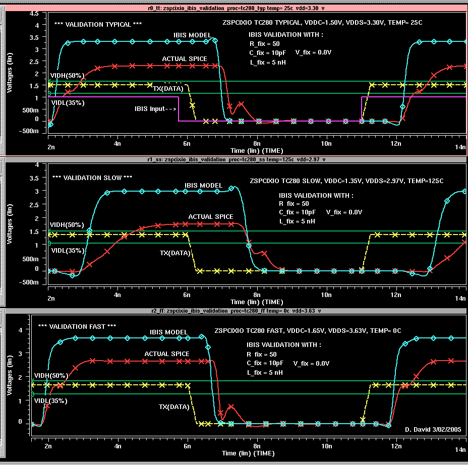
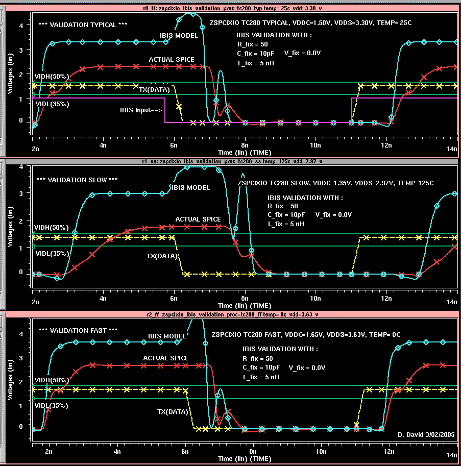
Hello experts:

I am trying to validate a PCI-X IBIS model using HSPICE simulation comparing
the IBIS model to actual circuit netlist.

The first gif file shows the Rising & Falling waveforms that were characterized
for IBIS, both with a load of 50-ohm to Ground (0.0V).  I also included two more
Rising & Falling waveforms with load of 50-ohm to VDD.

Below is how I intsantiated the IBIS model in HSPICE (version W-2004.09).
The ramp_rwf & ramp_fwf are set to "1", telling the simulator to only look
at the first Rising & Falling waveforms, which have load of 50-ohm to Ground.

For the actual circuit, I have it set up with same waveform fixture parameters
used to model IBIS, also with load of 50-ohm to Ground.

As seen in first plot for IBIS model, the red line (actual circuit) in 2nd plot
does not reach VDD since I have load of 50-ohm to Ground in all cases.

However, no matter what I do, the IBIS waveforms always come out with full
logic swings (0.0 - 3.3V) even though my Rising & Falling waveform in IBIS
file are quite below VDD (actually 2.285V,1.757,2.653 for typ/min/max).

If you have any suggestions, please let me know if I may have overlooked anything
in setup that would cause this mismatch with IBIS model having full logic swing.
I also have "nd_in" (IBIS input) driven into IBIS model with 1pS slew and 0-1V
levels.

---- IBIS instance used in my HSPICE test bench : ----

B_IO  nd_pu  nd_pd  nd_out nd_in nd_en v_out_of_in  nd_pc  nd_gc
+ file  = '../ibis_models/zspcixio_raw.ibs'
+ model = 'ZSPCIXIO'
+ typ   = 'typ'        $ choose typ = [typ/min/max]
+ buffer= input_output
+ power = on           $ [on] connects nd_pu/nd_pd/nd_pc/nd_gc to power sources in ibis.
+ interpol = 2         $ 1=linear interpolation, 2=quadratic bi-spline interpolation.
+ ramp_rwf = 1         $ Rising:  0-use ramp, 1-use 1st waveform data, 2=use two waveforms
+ ramp_fwf = 1         $ Falling: 0-use ramp, 1-use 1st waveform data, 2=use two waveform
----------------------------------------------------------------------------------------

Best Regards,
Doran David
 ________________________________________________________________
| Circuit Simulation                    | Work : (972) 246-5334  |
| Toshiba America Electronic Components | Cell : (214) 995-9785  |
| 740 E. Campbell Rd. Suite 620         | Fax  : (972) 235-4114  |
| Richardson, TX  75081                 | Email: davidd@taec.com |
|_______________________________________|________________________|


|------------------------------------------------------------------
|For help or to subscribe/unsubscribe, email majordomo@eda.org
|with just the appropriate command message(s) in the body:
|
|  help
|  subscribe   ibis       <optional e-mail address, if different>
|  subscribe   ibis-users <optional e-mail address, if different>
|  unsubscribe ibis       <optional e-mail address, if different>
|  unsubscribe ibis-users <optional e-mail address, if different>
|
|or email a written request to ibis-request@eda.org.
|
|IBIS reflector archives exist under:
|
|  http://www.eda.org/pub/ibis/email_archive/  Recent
|  http://www.eda.org/pub/ibis/users_archive/  Recent
|  http://www.eda.org/pub/ibis/email/          E-mail since 1993