Date: Fri Nov 17 2006 - 06:30:07 PST
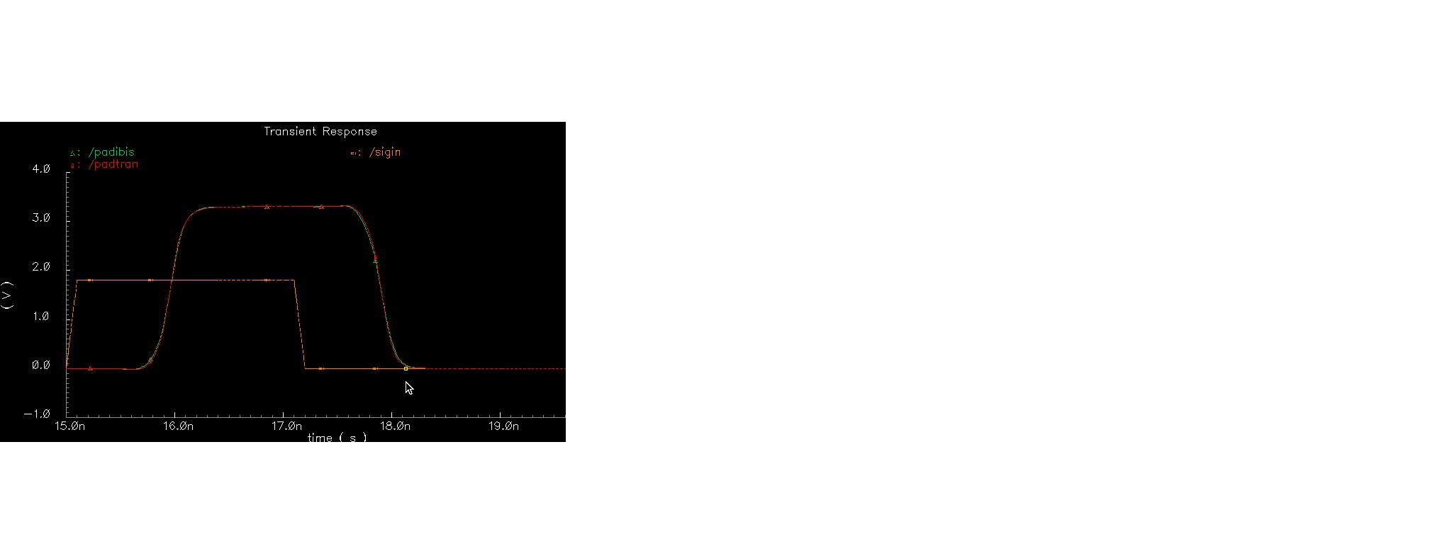
 Fabio,

It is good that you are taking the time and effort to verify your completed
model against simulation (A lot of vendors don't).  You should be able to
get a MUCH better match than that, however.  In general, the DC high and low
levels should be within a few mV of simulation, and the edges should be
quite close as well.

I'm attaching a sample waveform that I obtained.  It shows the square wave
input to the driver (orange), and the green signal is the output of the ibis
model and red signal is the output of the transistor model.

Check that you are using identical output loading in both simulations.
Start by using just a resistive load to ground, and no RLC package
parasitics (It looks like you have something more complex based on the
amount of overshoot and ringing).  I've used spectre and hspice to simulate
ibis models, and they ignore package parasitics in the ibis model, so I just
put a resistive load to ground on the output of the transistor model and the
ibis model.  I don't know if Eldo ignores this information as well, but if
in doubt, just set it to zero in the ibis file.  This will help to ensure
that you are comparing both simulations with identical loads.  However, this
should not cause the huge DC offset problems that you have (unless your
parasitics are way too large).  Chances are that there is something wrong in
your clamp data and pullup/pulldown data.

Hope this helps...

Dwayne Johnson
IC Design Engineer
Gennum Corporation,
4281 Harvester Road
Burlington, Ontario, Canada
L7L 5M4

website: www.gennum.com
email: dwayne_j@gennum.com
phone: 905-632-2999 x 2640
fax: 905-633-8105


-----Original Message-----
From: owner-ibis-users@eda.org [mailto:owner-ibis-users@eda.org] On Behalf
Of Fabio BRINA
Sent: Friday, November 17, 2006 4:39 AM
To: ibis-users; ibis-info
Subject: [IBIS-Users] sim results


Hi experts,

I have extracted ibis model by  s2ibis3 tool, the ibisck don't reveal any
errors or warnings.
But when I compare the ibis model simulation with the original Eldo
simulation , the width of the ibis output is real smaller, and the initial
point is 1.7V instead of 0V. (see figure) Which is, in your opinion,  a
possible problem?
I have to throw away the .ibs model? (I hope no!)

Thanks all
Fabio


--------------------------------------------------------------------
|For help or to subscribe/unsubscribe, e-mail majordomo@eda-stds.org
|with the appropriate command message(s) in the body:
|
|  help
|  subscribe   ibis       <optional e-mail address, if different>
|  subscribe   ibis-users <optional e-mail address, if different>
|  unsubscribe ibis       <optional e-mail address, if different>
|  unsubscribe ibis-users <optional e-mail address, if different>
|
|or e-mail a request to ibis-request@eda-stds.org.
|
|IBIS reflector archives exist under:
|
|  http://www.eda-stds.org/pub/ibis/email_archive/ Recent
|  http://www.eda-stds.org/pub/ibis/users_archive/ Recent
|  http://www.eda-stds.org/pub/ibis/email/         E-mail since 1993