Syed B. Huq, National Semiconductor Corp.
Electronic Design Dec2nd 1996
High-performance systems that incorporate features such as parallel processing or other complex functions, and operate at high clock speeds, place tough demands on the design of the boards thta hold the circuits. Dealing with issues such as tight clock distribution and high-speed interfaces to meet forthcoming bandwidth-hungry applications are a few of the key challenges designers are facing today.
Therefore, the ability to simulate a design has become a critical factor in the success of a project. Design cycle times are getting shorter, and in many cases, the cost to build a prototype is no longer feasible. To solve these problems, designers need device models to perform intensive and accurate board-level simulation, since this capability has become a requirement rather than an option.
Now, the challenge is: How do you perform the board-level simulation if all the models for the board are not available ? Thus far, SPICE has been the only consistent method by which circuit-level models are created today. However, semiconductor vendors that create the models for their chips could not readily give these models out since they often contained proprietary process and circuit information.
There is , however a solution for modeling thanks to the creation of the I/O Buffer Information Specification(IBIS). This specification is a fast and accurate behavioral method of modeling input/output buffers based on V/I curve data derived from measurements or full circuit simulation. It uses a standardized software-parsable format in the form of an ASCII file to store the behavioral information needed to model device characteristics of integrated circuits. IBIS is compatible with virtually every simulator and EDA tool existent, and is supported by a wide range of industry leaders.
Why IBIS ?
The IBIS model file does not require proprietary information about the modeled circuit since no process or circuit design information is disclosed. On the other hand, a SPICE model can disclose substantial information that semiconductor vendors consider to be confidential, circuit nodal connections and process parameters, for example. The IBIS models are also accurate since nonlinear aspects of I/O structures, as well as package parasitics and ESD structures, are considered in the model parameters.
Furthermore, since IBIS is behavioral, the simulation time for a model can run 25X faster than a structural model such as used in SPICE. In addition, IBIS does not have nonconvergence issues such as encountered in SPICE models, and can run on most industry-wide platforms since most EDA vendors support the IBIS specification. In contrast, SPICE models from one vendor may not work on other simulators since each commercial version of SPICE has deviated slightly from the original SPICE2G.6.
Tool vendors have made improvements on the post processor in trying to differentiate their tools from other SPICE tools. Some semiconductor vendors also have their own internal SPICE engine that can be incompatible with commercial SPICE engines. By providing one IBIS model, a semiconductor vendor can be sure that it will work on most EDA tools(both SPICE and non- SPICE-based).
One of the most popular uses of IBIS is for signal integrity analysis of systems boards. The models are easy to create since they can be made from bench measurements or from simulation data. Simulations of a few nets on a PCB can be done with SPICE, but as the number of nets increase and the PCB gets more complex, it is impossible to simulate the entire board on SPICE. A fast, accurate behavioral method like IBIS is ideal.
Learning To Use IBIS
To use IBIS, a model must be created(a fairly simple procedure). First, examine the behavioral block diagram of an input/output buffer structure and put the various blocks in IBIS notation(Figure 1). The model of the I/O blocks consists of many small elements, ranging from package factors to clamping elements to buffer characteristics(thresholds, rampup and rampdown, and pullup and pulldown preformance).
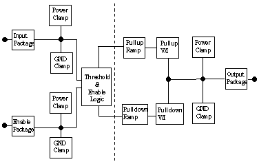
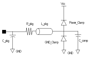
Information is needed to model the input structure appears similar to a transmission-line model, with package capacitance, resistance, lead inductance, and I/O-pad capacitance all affecting the input signal(Figure 2a). C_pkg, R_pkg and L_pkg are the package parameters. Power_Clamp and GND_Clamp defines the ESD structures on the inputs, while C_comp is the input capacitance of the input pin. The V/I curve data defines these clamp structures.
Information needed to model the output structure follows a similar structure, but in reverse(Figure 2b). Pullup defines the Voh/Ioh, Pulldown defines the Vol/Iol and Ramp defines the dV/dt of the device. The Pullup and Pulldown data are created from the V/I curves. The remaining parameters are similar to the input structure except that they define the package parasitics of the output pin, as well as the output capacitance of the output pin.
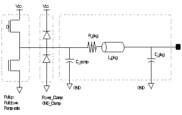
The Pullup and Power_Clamp data are “ Vcc relative”, meaning that the voltage values are referenced to Vcc and not ground. Vcc relative data is necessary for the simulator since the Pullup structure depends on the voltage between the output and Vcc, and not the voltage between the output and ground pin. The IBIS standard also supports multiple types of output structures. Refer to the specification for more details.
Once all the necessary V/I and other parameters are obtained through measurements, simulation, or provided by the chip vendor the model can be generated(Figure 3). First the interconnect engineer creates the IBIS ASCII file following the format defined in the IBIS standard. The ASCII model file is then checked by the “Golden Parser” for possible syntax errors. If passed, the model is then imported into a simulator and validated for accuracy. Now the model is ready for use.
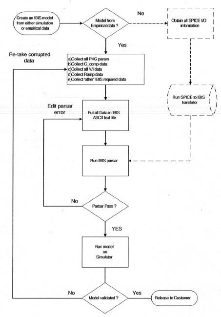
IBIS models can be generated from SPICE simulations or from actual empirical data. North Carolina State University has written a SPICE-to-IBIS converter program. A user can download the shareware program from the ERL(Engineering Research Lab) web site and create IBIS models.
The program, s2ibis2, creates an IBIS model file that conforms to the IBISv2.1 specification and uses HSPICE, PSPICE, SPICE2, SPICE3 or Spectre outputs as the source file. The s2ibis2 source code, as well as the executable files for various computing platforms, are available from the web site. The source code also can be modified to work with proprietary SPICE engines. The first generation of the converter is called s2ibis conforming to the IBISv1.1 specification, and is also available on the web site.
A handy utility for IBIS, s2iplt is a PERL (Pattern Extraction and Report Language) script that reads through an IBISv2.1 or lower version model file calling gnuplot (a UNIX utility) to plot each V/I table. This is a handy utility for IBIS model verification. The V/I plots can give a good indication if something is wrong with the data or data entry.
Modeling At Ground Zero
IBIS models, of course, also can be created from empirical data. To do that, first, identify the number of input and output models that are needed. If certain input/output pins have the same characteristic behavior, they can be grouped toether into one model. The Power and GND pins are not modeled by IBIS.
In the model, IBIS requires a number of essential parameters and also gives the user the opportunity to include several optional parameters. These are all detailed in the full specification. To create the model, the following parameters are required.
C_comp: Device input or output pad capacitance.Before the first measurements are taken, however, there are certain IBIS required formats that must be followed. The IBIS model specifies a range that an input and output structure must be swept. In most cases, these required ranges exceed the Absolute Maximum rating (ABS Max rating) of the device. But the model developers should not exceed the manufacturer’s ABS Max rating since that would overstress the die, potentially causing severe damage to the die corrupting the data. The input/output structure should be swept to the point where the structure starts to break down. Take all the data to this end range value, then extrapolate the linear region of the data to the IBIS specified range. Extrapolation of data to the end point is acceptable by the IBIS forum.R_pkg, C-pkg, L_pkg: Lumped value of package parameters.
R_pin, C_pin, L_pin: Pin package parameters
[Pulldown]: V/I table for Vol/Iol
[Pullup]: V/I table for Voh/Ioh
[GND Clamp]: V/I table of the ESD structure (low side).
[Power_Clamp]: V/I table of the ESD structure (high side)
[Rising Waveform]: Describes the waveshape of the rising waveform through V/T table.
[Falling Waveform]: Describes the waveshape of the falling waveform through V/T table.
dV/dT_r, dV/dT_f: Defines the ramp rate for rising and falling transitions.
Some simulators may not be able to extrapolate correctly. By providing the data across the entire range, the model is more usable across various SPICE and non-SPICE based simulators. This further gurantees the model to work on various tools supporting IBIS.
After extrapolation, it’s a good check to plot the data points to make sure linearity is maintained. A graphical plot may show abnormalities more readily then trying to go through a long listing of V/I data points.
When collecting the empirical data, the following ranges, as defined in IBISv2.1 should be used (see table below)
			Ranges Defined in IBISv2.1
		------------------------------------------
		Keyword		Low Limit	High Limit
		------------------------------------------
		[Pulldown]	-Vcc		+2Vcc
		[Pullup]	-Vcc		+2Vcc
		[GND Clamp]	-Vcc		+Vcc
		[Power Clamp]	+Vcc		+2Vcc
		------------------------------------------
As mentioned earlier, the [Power_Clamp] and [Pullup] structures are always referenced to Vcc. This means that once the V/I data is collected, the voltage table needs to be adjusted (offset) by using the following formula:
This can be done on a spreadsheet once all the datapoints are collected. Only the voltage table is adjusted. The current table remains unchanged.
Even though a floating power supply can be used to offset the Vcc and take measurements relative to Vcc, this is not recommended because serious damage can occur to the instrument if it is improperly connected.
To perform the actual data collection for ac (timing) and dc (static) testing, there may exist, or one can assemble, a bench fixture that can be used for all types of testing. An ac jig requires a 50 Ohm termination on input pins to effectively terminate the 50 Ohm source (a signal generator) that drives the input.
When testing dc parameters using the same jig, make sure to remove the termination values from the input pins. If the terminators are not removed a “constant slope”(resistor) appears on a curve tracer when it sweeps the input structures, thus invalidating the results.
All jigs have a distributed capacitive load associated with them. This can easily be 6 to 8pf based on the size of the jig. The user needs to know this jog capacitance value during model validation on a simulator. A bare board’s jig capacitance value can be measured using an LCR meter.
To measure the C_comp value, designers have several choices: The IEEE1194.1 standard (Electrical Characteristics of Backplane Transceiver Logic Interface Circuits) specifies the TDR (time domain reflectometry) method. This method is an approximation only. It compares the reflection profile of known capacitor values to the reflection profile of the device under test.
When performing this test, a TDR pulse is launched into the pin under test. The device-under-test (DUT) pin should be exposed and not inside a bench test socket and the device should be powered off. The fast (typical 35 to 45 ps) incident edge from TDR will encounter package and bonding discontinuities and reflect back from the device pin.
Since a capacitor does not allow an instantaneous change in voltage (I=CdV/dT), the reflection profile appears momentarily as a short and then rises back again. This “dip” on the reflection profile is a combination of package capacitance and device capacitance. This magnitude of the ‘dip’ can then be compared to known capacitor value (same TDR launch on the known capacitor). The value of the package capacitance must be extracted from this measurement to get a true C_comp measurement.
A more accurate measurement can be made using the Tektronix IPA510 (Interconnect Parametric Analyzer). The IPA510 uses a Z-profile algorithm to filter “ghost” reflections casused by the multiple reflections from various discontinuities. This Z-profile is then processed by the DSP software to extract the various Z, td, L and C values of the device under test.
The IPA510 also can be used to extract various package parameters as required by IBIS standard. The JEDEC JC-15 committee details how package parameters are to be measured. This, however, is not a trivial task, and it is recommended to go back to the semiconductor vandor to obtain package parameters.
Pick Instruments Wisely
Collecting the data from many test points can be a difficult task to perform. To speed things up, there are several off-the-shelf instruments and software packages that can be used to automate some of the data gathering and store IBIS related V/I data in ASCII format. Various choices exist from a number of vendors, and all can be used to take IBIS modeling data. Each instrument has its own merits and depending on the cost, systems can range from minimal automation to fully automated.
The TEK370A digitizing curve tracer from Tektronix is a programmable curve tracer that can readily perform V/I measurements. By networking the curve tracer to a computer, V/I data collection can be highly automated. The local/remote mode lets the user switch back and forth from automated to manual mode for verification purpose.
From Hewlett-Packard, the HP4142B modular dc source/monitor is similar to a Curve Tracer and uses menu driven commands to setup the tests. The HP4142B can plot and save data as required. This also is a handy tool if automated measurements are made through a GPIB capable host computer.
One software package that runs over that GPIB connection comes from Metrics. This software includes various driver programs for the instruments such as the TEk370A and the HP4145. By using the Metrics software on a PC with GPIB capability, a user can network the bench measurement equipment to the PC and data collection procedures.
The Metrics software does a quick sweep (single-shot) and collects the data. Data can then be plotted by the software, and is saved in an ASCII file in the VI format as required by IBIS.
Another option is the Kiethley220, a programmable current source that can also be tied to a GPIB networked PC. It should be noted that the DUT can heat up as the PC executes read/write sequences for each data point. Thermal feedback can alter the accuracy of the data being taken. Thus, thermal effects caused by the latency involved in executing GPIB read/write commands must be taken into account.
Another tool, the Interconnect Parametric Analyzer (IPA510), uses a TDR methodology along with DSP software to extract various interconnect models based on reflection profiles. This can be used for package parasitic measurements or to collect input/output capacitance values of semiconductor devices.
To perform the measurements the sequence of operations is relatively simple. For instance, to measure [GND_Clamp] and [Power_Clamp] for the input model use the following sequence:
(a) Apply power to the device.
(b) Connect the “collector” from the curve tracer to the input pin under test.
(c) Tie the “emitter” on the curve tracer to ground.
(d) Sweep the input structure from 0.0V towards negative voltage to the point the clamp structure turns ON to capture the [GND_Clamp] values and sweep the input from 0.0V to positive voltage to the point where the clamp structure turns ON to capture the [Power_Clamp] data. Sweeps can be done on both clamp structures simultaneously to the point where breakdown first starts to occur.
(e) STOP the sweep and collect the V/I data. As explained earlier, extrapolation should be used to extend the data to the IBIS required range.
Note that on an automated bench setup, if the current values are very small (~e-12), the resolution of the bench equipment may give positive and negative values of current for each voltage step until the value of the current increases significantly. Such data can violate IBIS rules for monotonacity. To compensate, the user can manually zero out the current readings. This effect can be experienced when sweeping the power clamp structure from 0.0 to 5.0V. Typically, the current in this region is very small - just at the point that the diode starts to conduct.
To measure [Pullup] and [Pulldown] for the output model, a simple procedure also can be set up. In a device datasheet, [Pullup] is referred to as Voh/Ioh data, and [Pulldown] is referred to as Vol/Iol data. The measurement method is similar to [Power_Clamp] and [GND_Clamp] measurements.
(a) For a three-state output, the output [Power_Clamp] and [GND_Clamp] values should be measured with the output in its high impedance state. That isolates the [Pulldown] and [Pullup] data from the [Power Clamp] and [GND Clamp] V/I data. The [Pulldown] and [Pullup] data must represent the difference of the three-state and the enabled buffer V/I data. Such a requirement enables the simulator to sum the curves without the danger of double counting. The user must then force the device into a “High” state for [Pullup] data and into a “Low” state for the [Pulldown] V/I data.
(b) For non-three-state devices, the [Pulldown] and [Pullup] data will contain the effects of the ESD structures ([Power Clamp] and [GND Clamp]). In this case, there is no need to create clamp V/I tables for the clamp structures.
(c) Always plot the V/I tables to see if there are any anomalies due to possible data corruption.
The only ac measurement required for IBIS modeling, the dV/dt_r and dV/dt_f parameters also can be done with the automated equipment. The tests are similar to tests that perform risetime or falltime measurements for digital devices. This test requires only one datapoint measured between the 20% to 80% voltage value and the time value is recorded to get the ramp rate. The ramp rate should be measured with no loading on the output structure. A user should employ a high bandwidth oscilloscope with a low capacitance probe to avoid loading effects. One such scope, the Tektronix 11801B (20 GHz) series with SD-14 probes (3 GHz), can readily handle the measurements.
Measuring the [Rising Waveform] and [Falling Waveform] values can be done by modeling the Gradual Turn On circuits (GTO) by using the assigned keywords. GTO circuits can be found in GTL, Crossvolt and other devices. The Tektronix IPA510 along with the 11801B scope setup can be used to capture the [Rising Waveform] or the [Falling Waveform] in an ASCII V/T table format as required by the IBIS standard. The Docuwave software from Tektronix also can be used to create a .CSV file that can be read into an Excel spreadsheet. The .CSV file again saves the waveform data in an IBIS required V/T table.
Handling Model Files
The IBIS standard specifies the creation of MIN, TYP and MAX models. It is difficult to take MIN, MAX data over process corners and temperature ranges, and such measurements can be best done by the respective semiconductor vendors. A TYP model can be created by an end user from the guidelines previously described. A DOS or UNIX text editor may be used to create the IBIS ASCII model file. The UNIX format is the preferred format but whichever is used, the model should always be checked by the parser to ensure IBIS compatibility.
The IBIS parser test uses the Golden Parser to make sure the model file conforms to the IBIS specification. The Parser does not indicate if you forgot to insert the proper ‘units’, but it is robust enough to catch various IBIS specification violations. To envoke the Parser, just type:
The Parser can run on various platforms and can be downloaded for free from the web site referenced at the end of the article.
The results of all the data collection and parsing is an ASCII table file that includes all the data points required to construct the model. Furthermore, all models must be validated for accuracy. This can be done by simulating the model with a known load and comparing the simulated data to actual bench measured data under similar loading conditions. Rise and fall times are some of the parameters that should be validated. If the IBIS model is generated from bench measurement, the measured and simulated data will match perfectly.
Syed B. Huq is a Staff Applications Engineer for the Interface Products Group, and has been working at National Semiconductor for nine years. He also is involved with signal integrity analysis/simulations, IBIS device modeling and Interconnect model extraction. He holds a BS degree in Electrical Engineering from Southern Illinois University, Syed is presently Vice chairman of the ANSI/EIA-656 IBIS committee.
References
IBIS:I/O Buffer Information Specification Overview, Intel Corp., Hobbs, W., Muranyi, A., Rosenbaum R., Telian, D.
vhdl.org:(198.31.14.3) has been a central location to find various IBIS related information. This includes: Models, Golden Parser, BIRD(Buffer Issue Resolution Documents), Summit information, and a participating company roster listing. This is an anonymous ftp site and anyone can log on as anonymous and user their E-mail ID as a password. Dial up modem access also is available at (415)335-0110
ANSI/EIA-656: This IBIS web site serves as a central location that will continually provide various tools and resources in helping create IBIS models. IBIS related articles, FAQ (Frequently Asked Questions), Hypertext links to information on vhdl.org, Virtual Poster pages with hot links to member companies are some of the items available through this web site.
North Carolina State University: The University provides SPICE-to-IBIS translator tools from their site.
Hyperlynx: This company provides a tool called ‘Visual IBIS Editor’ that can be used to edit and plot IBIS models on a PC. The tool also supports syntax validation and has general template files for both v1.1 and v2.1. Visual IBIS Editor can run on Windows95, WindowsNT, Windows3.1 and Windows for Workgroups. Follow the directions provided and download this tool from their web site.
Semiconductor vendors providing models today:
National Semiconductor provides IBIS models for various products that can be downloaded from their web site. Check the ANSI/EIA-656 web site under Models for other semiconductor companies that currently provide IBIS models.
How to join the reflector or ANSI/EIA-656:
ibis-request@vhdl.org: To join, change, or drop from either the IBIS open forum reflector ibis@vhdl.org, the IBIS users group reflector ibis-users@vhdl.oeg or both. You must state your request.
ibis-info@vhdl.org: To obtain general information about IBIS, ask specific questions for individual responses, and to inquire about joining the EIA-IBIS open forum as a full member.
ibis@vhdl.org: To send a messge to the general IBIS open forum reflector. This is used mostly for IBIS standardization business and future IBIS technical enhancements.
ibis-users@vhdl.org: To send a message to the IBIS users group reflector. This is used mostly for IBIS clarifications, current modeling issues, and general user concerns.
ibischk-bug@vhdl.org: To report ibischk2 parser bugs. The bug report form resides on vhdl.org in /pub/ibis/bugs/bugform.txt along with reported bugs.
Instrument/Software suppliers:
Metrics Technology
417 Tramway NE, Suite#2
Albuquerque, NM 87123
(505)299-9591 or (800)398-1490
Fax(505)275-6261
National Instruments with LabVIEW
(800)433-3488 or (512)794-0100
ftp site at: ftp.natinst.com
Login: anonymous
Password: your E-mail ID
Look under  /support/labview/windows/instruments/lv30/gpib
P.O Box 500
Beaverton, OR 97077-0001
(800)835-9433
28775 Aurora Rd
Cleveland, OH 44139
(800)552-1115