Date: Sun Aug 02 2009 - 00:35:07 PDT
Hi all.

Good morning.

I had make an IBIS file that contain an input pin.

The gnd clamp ranges are from -vcc to vcc.

The power clamp ranges are from vcc to 2vcc (relative to gnd).


This pin should be with ODT of 50 ohm.

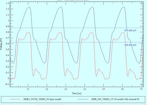
When we trying to simulate this pin (we are using allegro simulator). We got
the next wave:


The blue is the graph of the pin when adding external resistor and the red
is without.

The problem is that the red graph D.C voltage is too low.


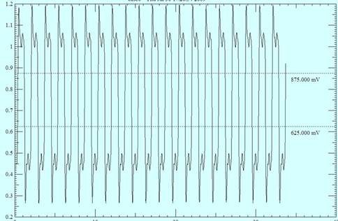
When we are taking the same IBIS file and adding the power clamp more points
so it now from 0 to 2vcc (relative to gnd), instead of vcc to 2vcc.

We receive better results (without external resistor):


So my question, is, why the power clamp range impact the results?

In the IBIS cook book it's written that a range of vcc should be enough.


Maybe it's a problem with the simulator?


Thanks in advance.


Kobi.


--
This message has been scanned for viruses and
dangerous content by MailScanner, and is
believed to be clean.


--------------------------------------------------------------------
|For help or to subscribe/unsubscribe, e-mail majordomo@eda-stds.org
|with the appropriate command message(s) in the body:
|
|  help
|  subscribe   ibis       <optional e-mail address, if different>
|  subscribe   ibis-users <optional e-mail address, if different>
|  unsubscribe ibis       <optional e-mail address, if different>
|  unsubscribe ibis-users <optional e-mail address, if different>
|
|or e-mail a request to ibis-request@eda-stds.org.
|
|IBIS reflector archives exist under:
|
|  http://www.eda-stds.org/pub/ibis/email_archive/ Recent
|  http://www.eda-stds.org/pub/ibis/users_archive/ Recent
|  http://www.eda-stds.org/pub/ibis/email/         E-mail since 1993

