Date: Fri Oct 15 2010 - 19:27:09 PDT
Todd,
You and the folks on the forum have been very helpful. I almost have this thing licked but I will be on vacation for a week. You may hear from me again, but thanks for your help!!
Best Regards,
Bonnie Baker
Sr. Applications Engineer
Texas Instruments, Tucson
5411 E. Williams
Tucson, Arizona 85711
(520) 750-2116 (work)
(520) 548-3111 (cell)
________________________________
From: Todd Westerhoff [mailto:twesterh@sisoft.com]
Sent: Friday, October 15, 2010 3:09 PM
To: tom@teraspeed.com; Baker, Bonnie; ibis-users@eda.org
Subject: RE: [IBIS-Users]: Using HSPICE to run IBIS model
Bonnie,
Doh! Tom is absolutely right about not needing a pullup resistor when extracting the I-V curves. I SAID it had been a long time, right?
Todd ;-)
________________________
Todd Westerhoff
VP, Software Products
SiSoft
6 Clock Tower Place, Suite 250
Maynard, MA 01754
(978) 461-0449 x24
twesterh@sisoft.com<mailto:twesterh@sisoft.com>
www.sisoft.com<http://www.sisoft.com>
________________________________
From: Tom Dagostino [mailto:tom@teraspeed.com]
Sent: Friday, October 15, 2010 5:22 PM
To: 'Baker, Bonnie'; 'Todd Westerhoff'; ibis-users@eda.org
Subject: RE: [IBIS-Users]: Using HSPICE to run IBIS model
Bonnie
The RLC circuit in his diagram is the package model.
You should not need a pullup resistor during the IV extractions. They should be done with no external devices attached to the buffer during the simulations. When the buffer is high there should be no current in the pulldown device and only current flowing when you have turned on the ground clamp with the sweep voltage about -0.6V or more. Most open drain buffer have no powerclamp. With the output in the low state you should see the normal FET IV characteristics. If you are seeing an offset you have some currents in one of your tables that should not be there.
The VT data should be extracted with a 50 Ohm resistor tied to 1.8V in your case. Yes the application resistor is likely to be 1K or greater but buffer will see a transmission line environment between the pin and the pullup resistor and it needs to drive that as the initial load.
Regards,
Tom Dagostino
Teraspeed Labs
13610 SW Harness Lane
Beaverton, OR 97008
503-430-1065
tom@teraspeed.com
www.teraspeed.com
Teraspeed Consulting Group LLC
121 North River Drive
Narragansett, RI 02882
401-284-1827
www.teraspeed.com
From: owner-ibis-users@eda.org [mailto:owner-ibis-users@eda.org] On Behalf Of Baker, Bonnie
Sent: Friday, October 15, 2010 1:15 PM
To: Todd Westerhoff; ibis-users@eda.org
Subject: RE: [IBIS-Users]: Using HSPICE to run IBIS model
Todd,
You are right. This is for an I2C device where the maximum clock rate is 3.4 MHz.
I am now running my ibis simulations with a termination resistor of 1k. Initially, I thought that the 1K termination resistor was taken care of by the model. This is not true!
In your circuit diagram below, I find it interesting the you have R1 at the far end of the termination circuit (R2, L1, and C1). I was simulating with R1 connected at the output of tsc2014_nokia_3.
I now have questions about how to generate the IBIS model properly.
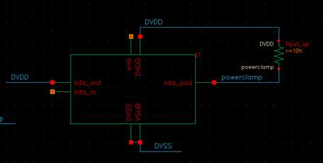
For I-V data collection
I am finding that I need to include a pull-up resistor in the circuit. If I don’t I have a very large offset error with my validation exercise. The circuit that I am using right now is:
[cid:image001.jpg@01CB6C9E.F593AE40]
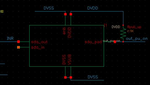
For V-t data collection
I am finding that I need to put a large Rfixture resistor. The circuit that I am using right now is:
[cid:image002.jpg@01CB6C9E.F593AE40]
With Rfixture equal to 10K.
Best Regards,
Bonnie Baker
Sr. Applications Engineer
Texas Instruments, Tucson
5411 E. Williams
Tucson, Arizona 85711
(520) 750-2116 (work)
(520) 548-3111 (cell)
________________________________
From: Todd Westerhoff [mailto:twesterh@sisoft.com]
Sent: Friday, October 15, 2010 6:27 AM
To: ibis-users@eda.org; Baker, Bonnie
Subject: RE: [IBIS-Users]: Using HSPICE to run IBIS model
Bonnie,
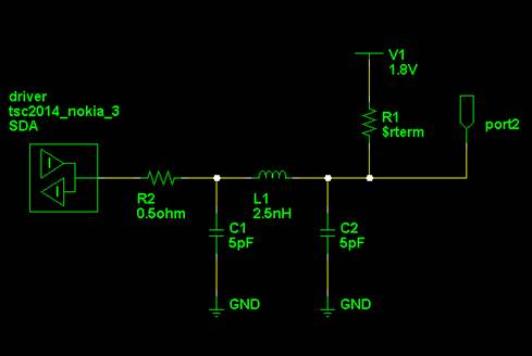
I took your model and ran it with and without a terminating pullup resistor. It behaved as we expected. I needed to use a relatively long data UI (15nS) to get a plot that showed the behavior I was seeing – I’m assuming this isn’t a very high speed device?
Here’s the circuit I simulated:
[cid:image003.jpg@01CB6C9E.F593AE40]
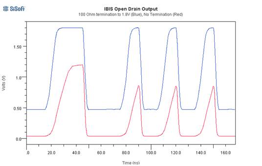
I used the 1.8V open_drain model and terminated it to 1.8V as shown. I used values of 100 ohm and 5M ohm for $rterm to illustrate the terminated and open circuit cases. I actually didn’t use HSPICE, not because that was difficult, but because I wanted to demonstrate the behavior you saw is expected and simulator independent.
The unterminated case displays poor switching behavior, the terminated case behaves as expected:
[cid:image004.jpg@01CB6C9E.F593AE40]
The question in my mind was – with no termination, why did the output rise at all? It turns out that the [GND Clamp] curve is always sourcing current (albeit a small amount), so once the pulldown device shuts off, the [GND Clamp] begins charging the output. The current is small enough that you need to leave the output essentially open to see it.
The [GND Clamp] curve looks incorrect to me, but I’d need to know more about the actual structure of the device to make that conclusion.
Hope that helps,
Todd.
________________________
Todd Westerhoff
VP, Software Products
SiSoft
6 Clock Tower Place, Suite 250
Maynard, MA 01754
(978) 461-0449 x24
twesterh@sisoft.com<mailto:twesterh@sisoft.com>
www.sisoft.com<http://www.sisoft.com>
________________________________
From: Baker, Bonnie [mailto:bonnie@ti.com]
Sent: Thursday, October 14, 2010 4:36 PM
To: Todd Westerhoff; 'Muranyi, Arpad'; ibis-users@eda.org
Subject: RE: [IBIS-Users]: Using HSPICE to run IBIS model
My Ibis file is attached to this message (that is if attachments come through).
Best Regards,
Bonnie Baker
________________________________
From: owner-ibis-users@eda.org [mailto:owner-ibis-users@eda.org] On Behalf Of Todd Westerhoff
Sent: Thursday, October 14, 2010 6:53 AM
To: 'Muranyi, Arpad'; ibis-users@eda.org
Subject: RE: [IBIS-Users]: Using HSPICE to run IBIS model
Arpad,
I think Doug Burns nailed it – no pullup on an IBIS open-drain output. The fact that the output is rising at all is interesting, but I agree with his assessment of leakage currents.
Todd.
________________________
Todd Westerhoff
VP, Software Products
SiSoft
6 Clock Tower Place, Suite 250
Maynard, MA 01754
(978) 461-0449 x24
twesterh@sisoft.com<mailto:twesterh@sisoft.com>
www.sisoft.com<http://www.sisoft.com>
________________________________
From: owner-ibis-users@eda.org [mailto:owner-ibis-users@eda.org] On Behalf Of Muranyi, Arpad
Sent: Thursday, October 14, 2010 1:06 AM
To: ibis-users@eda.org
Subject: RE: [IBIS-Users]: Using HSPICE to run IBIS model
Bonnie,
I was working at Intel when the B-element and its variants were
added to HSPICE, and I worked quite a lot with the developer to
help him to get it right. I tested a lot of his work before and
after it was released. The various buffer types were all working
correctly as far as I remember. Your problem description doesn't
give me all the details to be able to pinpoint the problem, but I
wonder how do you expect the signal to move up or down when the
buffer turns off its (only) transistor but your circuit doesn't
seem to have a resistive connection to GND or Vcc?
Arpad
=================================================================
________________________________
From: Xuefeng Chen [mailto:Xuefeng.Chen@synopsys.com]
Sent: Wednesday, October 13, 2010 11:48 PM
To: Baker, Bonnie; Muranyi, Arpad; ibis-users@eda.org
Subject: RE: [IBIS-Users]: Using HSPICE to run IBIS model
Hi Bonnie,
I am sure HSPICE supports all kinds of IBIS buffer types except external model of VERILOG-AMS or VHDL-A(MS).
From the mail without the ibis file, it’s hard to figure out the issue. Would you like contact HSPICE related AC or CAE for help.
Thanks,
Xuefeng
From: owner-ibis-users@eda.org [mailto:owner-ibis-users@eda.org] On Behalf Of Baker, Bonnie
Sent: 2010年10月14日 11:53
To: Muranyi, Arpad; ibis-users@eda.org
Subject: [IBIS-Users]: Using HSPICE to run IBIS model
I am using Hspice to run IBIS and comparing it to a Spice simulation. The Spice simulates the buffer well but the Hspice program is having problems. My buffer type is I/O_open_drain.
The circuit diagram is:
-------------
I/O / R=0.5 L=2,5e-9
Open- /-----------/\/\/\/\-------|------/\_/\_/\_/\---------|---------O output
Drain / | |
Buffer / --- ----
------------ --- C=1e-12 ---- C=5e-12
| |
GND GND
The I/O buffer is driven with a rail to rail input signal. The output signal does to reach the rail as expected. It actually looks like:
---------------------expected-output-high--------------------------------------------------
_______
_______/
_______/
_____/
___/
__/
_/
/
/
/
__/______________________________________________________
I expect
---------------------expected-and-actual-output-high--------------------------------------------------
/
/
/
/
/
/
/
/
/
/
/
__/______________________________________________________
It appears as if Hspice does not recognize the fact that this buffer is open drain.
Has anyone else experienced this and is the a work around?
The Hspice netlist is:
*
* HSPICED IBIS I/O open drain BUFFER TEST BENCH
* Temperature
.TEMP 27
* POWER SUPPLIES and SIGNAL VOLTAGES
VVCC VCC 0 DC=VCC
VGND GND 0 DC=GND
*PARAMETER DEFINITIONS
.PARAM GND = 0V
.PARAM VCC = VCC_typ
.PARAM VCC_typ = 1.8
* Simulation Options
.OPTIONS ACCT ACCURATE NOPAGE OPTS POST SCALE=1e-6
.OPTIONS METHOD=GEAR
*=========TRANSIENT ANALYSIS sim========
.TRAN 0.1e-9 13000e-9 START =0.0e-9
* TD
VIN_ibis IN_ibis GND PULSE VCC GND 0ps 0.01ns 0.01ns 149.99ns 300n
*******************AC LOAD**************
B_IO nd_pu nd_pd Out_ibis IN_ibis nd_en SDA_signal nd_pc nd_gc
+ file = 'tsc2014_nokia_3.ibs' model = 'SDA_1'
+ typ = typ power = on
+ buffer = 6
+ ramp_fwf=1 ramp_rwf=1
Rpcb Out_ibis n1_pcb 0.50
Lpcb n1_pcb OUT_pcb_ibis 2.5e-9
Cpcb n1_pcb GND 1e-12
Cpcbload OUT_pcb_ibis GND 5e-12
Bonnie
--
This message has been scanned for viruses and
dangerous content by MailScanner<http://www.mailscanner.info/>, and is
believed to be clean.
--
This message has been scanned for viruses and
dangerous content by MailScanner<http://www.mailscanner.info/>, and is
believed to be clean.
--
This message has been scanned for viruses and
dangerous content by MailScanner<http://www.mailscanner.info/>, and is
believed to be clean.
--
This message has been scanned for viruses and
dangerous content by MailScanner<http://www.mailscanner.info/>, and is
believed to be clean.
--
This message has been scanned for viruses and
dangerous content by MailScanner, and is
believed to be clean.
--------------------------------------------------------------------
|For help or to subscribe/unsubscribe, e-mail majordomo@eda-stds.org
|with the appropriate command message(s) in the body:
|
| help
| subscribe ibis <optional e-mail address, if different>
| subscribe ibis-users <optional e-mail address, if different>
| unsubscribe ibis <optional e-mail address, if different>
| unsubscribe ibis-users <optional e-mail address, if different>
|
|or e-mail a request to ibis-request@eda-stds.org.
|
|IBIS reflector archives exist under:
|
| http://www.eda-stds.org/pub/ibis/email_archive/ Recent
| http://www.eda-stds.org/pub/ibis/users_archive/ Recent
| http://www.eda-stds.org/pub/ibis/email/ E-mail since 1993