Subject: RE: [IBIS-Users] IBIS Specification Question
From: James_R_Jones@Dell.com
Date: Wed Jul 24 2002 - 06:40:40 PDT
For what it's worth, I've seen some IBIS models contain both power clamp and
and pull up data in the pull up curve. I would think that this would
accurately represent the superposition of the two. If you want to separate
the two, I would think that the power clamp should include only the effects
of the diode, and the pull up should contain only the effects of the
transistor.
Hope this helps,
JR
-----Original Message-----
From: Shee Kian Wong [mailto:SKWONG@altera.com]
Sent: Wednesday, July 24, 2002 2:47 AM
To: ibis-users@eda.org
Subject: [IBIS-Users] IBIS Specification Question
Hi all,
I'm currently studying the IBIS Specification. I have some ambiguities about
the I/O Buffer Modeling Cookbook prepared by IBIS Forum.
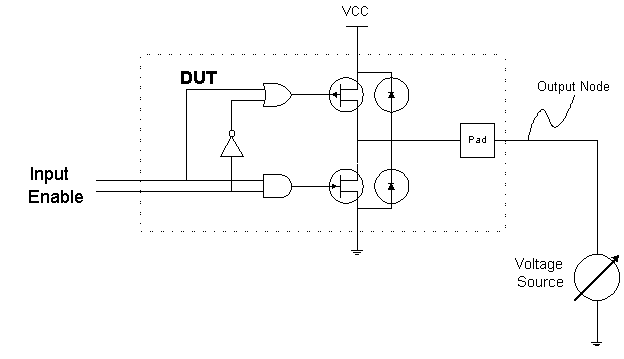
A typical simulation setup for an output or I/O buffer is given in Page 8 of
the Cookbook, as shown below:
I understand that for an I/O (3-stateable) buffer four sets of I/V curves
are required; one with the pulldown transistor turned on (output in the low
state) (pulldown curve), one with the pullup transistor turned on (output in
the high state) (pullup curve), and two with the output in a high impedance
state (power clamp and ground clamp curves).
For example, when we want to enable the pullup transistor, we would supply
ENABLE pin with vcc (logic 1) and INPUT pin with 0 (logic 0). However, when
the voltage source sweeps in the range of -vcc to 0, the NMOS will be turned
on as well. This is due to the fact that Vpad is smaller than Vgnd, then the
drain of the NMOS would be at the ground side. Since Vgs>0 (G=Logic 0,
S<logic 0), the NMOS is turned on.
Therefore, some ground clamp currents flow through the pulldown transistor.
Why the equation Vpullup(table) = Vpullup - Vpower_clamp does not take care
of the ground clamp current? Also, some current will flow through the pullup
transistor during this voltage sweep range, do we call it pullup current or
ground clamp current?
When the voltage source sweeps from vcc to 2*vcc, again, some current flow
through the pullup transistor. Do we call this current pullup current or
power clamp current?
The same thing occurs to pulldown I/V case.
There are no ambiguities for power clamp and ground clamp curves.
Please kind advice and correct me if I'm wrong.
Much appreciated,
Shee Kian Wong
Applications Engineer
Altera Corporation (M) S/B

|------------------------------------------------------------------
|For help or to subscribe/unsubscribe, email majordomo@eda.org
|with just the appropriate command message(s) in the body:
|
| help
| subscribe ibis <optional e-mail address, if different>
| subscribe ibis-users <optional e-mail address, if different>
| unsubscribe ibis <optional e-mail address, if different>
| unsubscribe ibis-users <optional e-mail address, if different>
|
|or email a written request to ibis-request@eda.org.
|
|IBIS reflector archives exist under:
|
| http://www.eda.org/pub/ibis/email_archive/ Recent
| http://www.eda.org/pub/ibis/users_archive/ Recent
| http://www.eda.org/pub/ibis/email/ E-mail since 1993
This archive was generated by hypermail 2b28 : Wed Jul 24 2002 - 07:02:56 PDT